

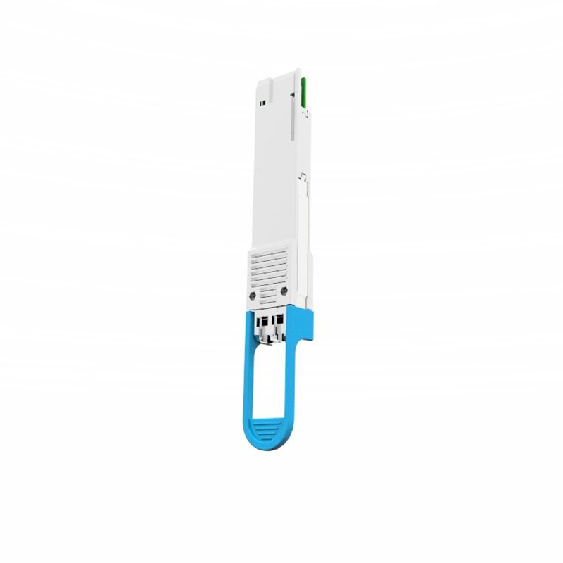
200G QSFP-DD LR4 Optical Transceiver HQSFPDD-2L2 LAN WDM DFB, PIN, 0~70℃
Features
● Hot-pluggable QSFP-DD MSA form factor
● Supports 212.5Gb/s aggregate bit rates
● Power dissipation < 10W
● Commercial case temperature range of 0°C to 70°C
● Single 3.3V power supply
● Maximum link length of 10km on Single Mode Fiber (SMF)
● Transmitter: Cooled 4 channels 200G PAM4 LAN WDM DML TOSA
● Receiver: 4 channels 200G PAM4 PIN ROSA
● 200GAUI-8 (or 200GAUI-4 ) Electrical Interface
● Duplex LC receptacles
● I2C Management Interface with DOM
Applications
● IEEE 802.3bs 200GBASE-LR4 Ethernet (PAM4)
General Description
Hi-Optel’s 200G QSFP-DD transceiver module is designed for use in 200G Ethernet interfaces over single mode fiber. It is compliant with both the QSFP-DD MSA and 200GBASE-LR4 specification. The central wavelengths of the 4 LAN WDM channels are 1295.56, 1300.05, 1304.58 and 1309.14 nm as members of the LAN WDM wavelength grid defined in IEEE 802.3ba. The high performance cooled LAN WDM DML TOSA transmitters and PIN-PD receivers provide superior performance for 200G Ethernet applications up to 10km links with FEC. Digital diagnostics functions are available via the I2C interface, as specified by QSFP-DD MSA. This product is intended to support data center applications.
Ordering Information
| Part Number | Description |
| HQSFPDD-2L2 | QSFP-DD 200GBASE-LR4 LWDM 10 km |
General Specifications:
| Parameter |
Symbol |
Min |
Typical |
Max |
Unit |
Note |
| Data Rate, all Lanes combined |
DR |
|
|
212.50 |
Gb/s |
|
| Data Rate, each Lane |
|
|
26.5625 |
|
Gb/s |
|
| Data Rate Accuracy |
|
-100 |
|
100 |
ppm |
|
| Link Distance |
D |
|
|
10 |
km |
Absolute Maximum Ratings:
Module performance is not guaranteed and reliability is not implied for any condition that beyond the operating range. Exceeding the limits below may damage the transceiver module permanently.
| Parameter |
Symbol |
Min |
Max |
Unit |
Note |
| Storage Temperature |
TST |
-40 |
+85 |
˚C |
|
| Operating Case Temperature |
TOP |
0 |
+70 |
˚C |
|
| Power Supply Voltage |
VCC |
-0.5 |
+3.6 |
V |
Recommended Operating Conditions:
| Parameter |
Symbol |
Min |
Typical |
Max |
Unit |
Note |
| Operating Case Temperature |
TOP |
0 |
|
+70 |
˚C |
|
| Power Supply Voltage |
VCC |
3.135 |
3.3 |
3.465 |
V |
Electrical Characteristics:
| Parameter |
Symbol |
Min |
Typical |
Max |
Unit |
Note |
| Power Supply Voltage |
VCC |
3.135 |
3.3 |
3.465 |
V |
|
| Power Supply Current |
ICC |
|
|
3 |
A |
|
| Power Consumption |
P |
|
|
10 |
W |
|
| Transmitter Characteristics (Module Output) | ||||||
| Differential Data Input Swing |
+/-TX_DAT |
20 |
|
1200 |
mV pp |
|
| Common mode Voltage |
VCM |
-350 |
|
2850 |
mV |
1 |
| Receiver Characteristics (Module Input) | ||||||
| Differential Data Output Swing |
+/-RX_DAT |
200 |
|
900 |
mV pp |
|
| Common Mode Voltage |
VCM |
-350 |
|
2850 |
mV |
1 |
| Common Mode Noise, RMS |
VNO |
|
|
17.5 |
mV |
|
Note: 1. Vcm is generated by the host. Specification includes effects of ground offset voltage.
Optical Characteristics:
| Parameter |
Symbol |
Min |
Typical |
Max |
Unit |
Note |
| Lane wavelength |
L0 |
1294.53 |
1295.56 |
1296.59 |
nm |
|
|
L1 |
1299.02 |
1300.05 |
1301.09 |
nm |
||
|
L2 |
1303.54 |
1304.58 |
1305.63 |
nm |
||
|
L3 |
1308.09 |
1309.14 |
1310.19 |
nm |
||
| Transmitter Characteristics (Per Lane) | ||||||
| Signaling Rate,each lane 26.5625 GBd PAM4 |
|
|
26.5625 |
|
GBd |
PAM4 modulation |
| Side Mode Suppression Ratio |
SMSR |
30 |
|
|
dB |
|
| Total Average Launch Power |
PT |
|
|
11.3 |
dBm |
|
| Average Launch Power per Lane |
PAVG |
-3.4 |
|
5.3 |
dBm |
|
| Extinction Ratio |
ER |
3.5 |
|
|
dB |
|
| Outer Optical ModulationAmplitude(OMA outer),each lane |
POMA |
-0.4 |
|
5.1 |
dBm |
|
| Difference in Launch power between any two lances(OMA outer) |
|
|
|
4 |
dB |
|
| Launch power in OMAouter minus TDECQ,each lane |
|
-1.7 |
|
|
dBm |
|
| Transmitter and dispersioneye closure for PAM4(TDECQ) each lane |
TDECQ |
|
|
3.2 |
dB |
|
| Average Launch Power OFFTransmitter, each Lane | Poff |
|
|
-30 |
dBm |
|
| Relative Intensity Noise | RIN |
|
|
-132 |
dB/HZ |
|
| Optical return loss tolerance |
|
|
15.6 |
dB |
|
|
| Transmitter reflectance |
|
|
-26 |
dB |
|
|
| Receiver Characteristics (Per Lane) | ||||||
| Signaling Rate,each lane |
|
|
26.5625 |
|
GBd |
PAM4 modulation |
| Signaling rate variation,each lane |
|
-100 |
|
+100 |
ppm |
|
| Lane wavelength range |
L0 |
1294.53 |
1295.56 |
1296.59 |
nm |
|
|
L1 |
1299.02 |
1300.05 |
1301.09 |
nm |
|
|
|
L2 |
1303.54 |
1304.58 |
1305.63 |
nm |
|
|
|
L3 |
1308.09 |
1309.14 |
1310.19 |
nm |
|
|
| Damage threshold,each lane |
Rdam |
6.3 |
|
|
dBm |
|
| Average receive power,each lane |
Rpow |
-9.7 |
|
5.3 |
dBm |
|
| Receive power (OMAouter),each lane |
ROMA |
|
|
5.1 |
dBm |
|
| Difference in receive power between any two lanes(OMAouter) |
|
|
|
4.2 |
dB |
|
| Receiver refletance |
|
|
|
-26 |
dB |
|
| Receiver Sensitivity(OMAouter),each lane |
SENeach |
|
|
-7.7 |
dBm |
|
| Stressed receiversensitivity(OMAouter),each lane |
|
|
|
-5.2 |
dBm |
|
|
Conditions of stressed receiver sensitivity test |
||||||
| Stressed eye closure for PAM4(SECQ), lane under test |
|
|
|
3.2 |
dB |
|
| OMAouter of each aggressor lane |
|
|
|
-1 |
dBm |
|
Transceiver Block Diagram
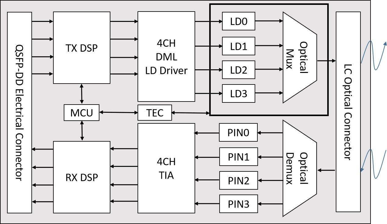
Figure 2. Transceiver Block Diagram
Pin Definition and Description
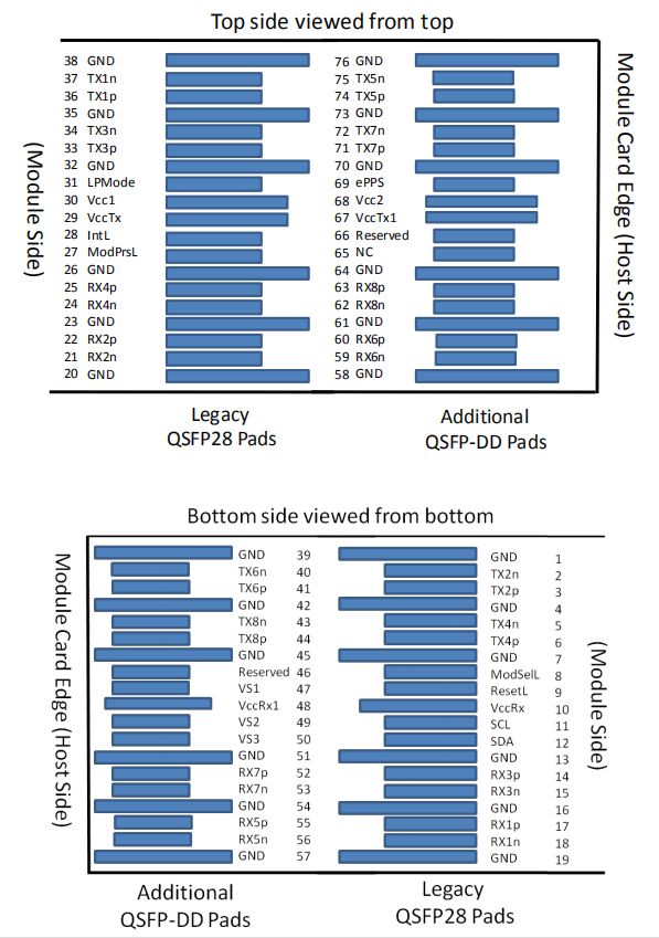
Figure 3. MSA compliant Connector(per QSFP-DD MSA)
Special Explanation on High-speed Electrical Interface
The electrical interface should comply with QSFP-DD MSA standard. The electrical interface
will vary by application, but the nominal signaling lane rate is 26.5625Gbit/s per lane and
comply with 200GAUI-8 (or 200GAUI-4 ) electrical interface specifications.
Table 7 The High-speed Signal Data Rate Supported by 200Gb/s QSFP-DD
|
Standard |
Descirption |
Nominal Bit Rate |
Units |
|
IEEE std-802.3bs |
200G Ethernet |
26.5625 |
Gbps |
Mechanical Specifications
This product is compatible with the QSFP-DD Specification for pluggable form factor modules.
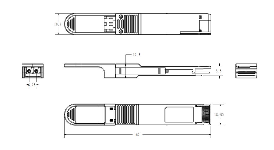
Figure 4. Mechanical Dimension (unit in mm)
ESD
This transceiver is specified as ESD threshold 500V electrostatic discharge for high speed pins and 2kV electrostatic discharge for all other electrical input pins, tested per JESD22-A114-B (Human Body Model). However, normal ESD precautions are still required during the handling of this module. This transceiver is shipped in ESD protective package. It should be removed from the package and handled only in an ESD protected environment.
Laser Safety
This is a Class 1 Laser Product according to EN 60825-1:2014. This product complies with 21 CFR 1040.10 and 1040.11 except for deviations pursuant to Laser Notice No. 50, dated (June 24, 2007).
Caution: Use of controls or adjustments or performance of procedures other than those specified herein may result in hazardous radiation exposure.
Revision History
| Revision | Date | Description |
| Preliminary | 2021/1/20 | Preliminary datasheet |