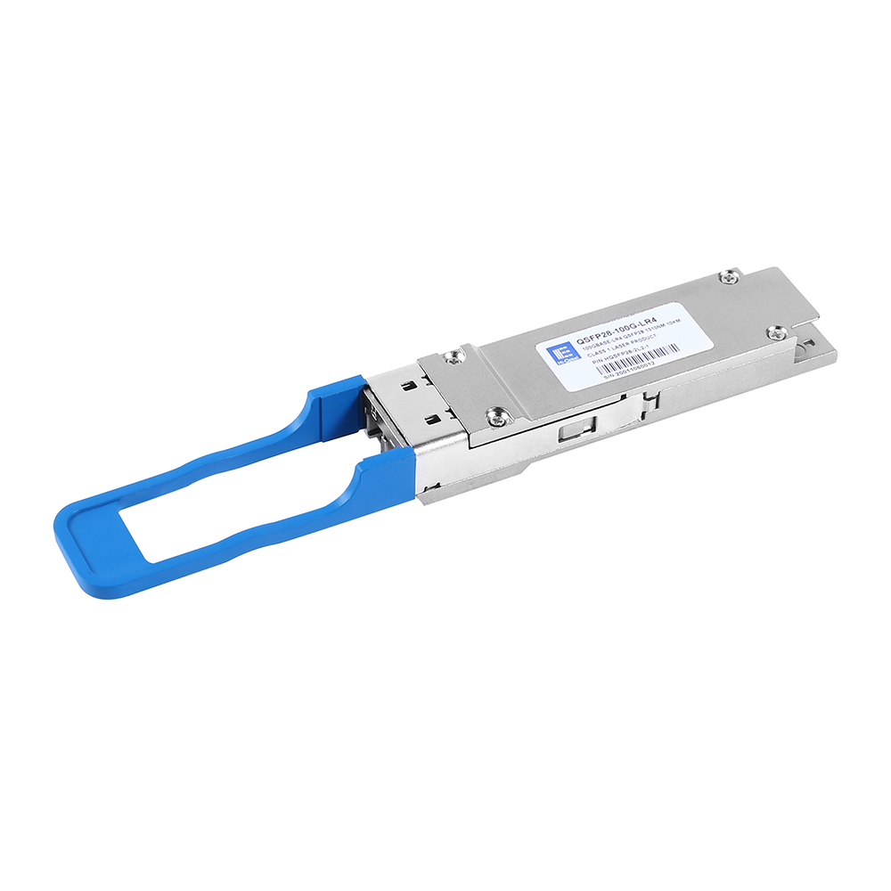
100GBASE-LR4 QSFP28 1310nm 10km Hi-Optel HQSFP28-2L2 module
Descriptions
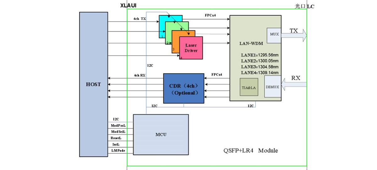
A block diagram of QSFP28 LR4 optical transceiver is shown below
Features
● Supports 103.1Gb/s aggregate bit rate
● 4x25.78Gb/s retimed electrical interface
● 4x25.78Gb/s DFB-based LAN-WDM transmitter and PIN/TIA receiver
● Maximum link length of 10km on Single Mode Fiber (SMF)
● Hot-pluggable QSFP28 footprint
● Duplex LC receptacles
● Single3.3V power supply
● Maximum power dissipation<3.5W
● RoHS-6 compliant and lead-free
● I2C management interface
● Case operating temperature: Commercial: 0°C to +70°C
Application
● 100GBASE-LR4 100G Ethernet
Compliance
● QSFP28 MSA.
● IEEE802.3bm and IEEE802.3ba
● SFF-8679
● RoHS
Digital Diagnostic Monitoring Interface
Digital diagnostics monitoring function is available on QSFP28 LR4. Real time monitoring includes module temperature, Module supply voltage, and monitoring for each transmitter and receiver channel.
The Memory Map for QSFP28 Module is used for serial ID, digital monitoring and certain control functions.
The interface is mandatory for all QSFP28 devices. The interface has been designed largely after the XFP MSA as defined in INF-8077i Rev.4.0. The memory map has been changed in order to accommodate 4 optical channels and limit the required memory space. The single address approach is used as found in XFP. Paging is used in order to enable time critical interactions between host and Module.
The structure of the memory is shown in Figure 30. The memory space is arranged into a lower, single page, address space of 128 bytes and multiple upper address space pages. This structure permits timely access to addresses in the lower page, e.g. Interrupt Flags and Monitors. Less time critical entries, e.g. serial ID information and threshold settings are available with the Page Select function. The structure also provides address expansion by adding additional upper pages as needed. For example, in table1 upper pages 01 and 02 are optional. Upper page 01 allows implementation of Application Select Table, and upper page 02 provides user read/write space. The lower page and upper page 00 are always implemented. Page 03 is required if byte 2, bit 2 in the lower page is low. See Table 39 for details regarding declaration of optional upper pages 01 and 02.
The interface address used is A0xh and is mainly used for time critical data like interrupt handling in order to enable a "one-time-read" for all data related to an interrupt situation. After an Interrupt, IntL, has been asserted, the host can read out the flag field to determine the effected channel and type of flag.
Table 1: Digital Diagnostic Memory Map (Specific Data Field Descriptions).
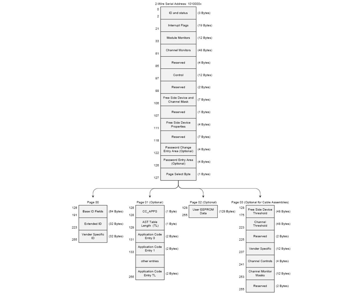
| Address | Description | Type | Passive Copper, Active Copper, Active Optical | Optical Module |
| 0 | Identifier (1 Byte) | Read-Only | R | R |
| 1-2 | Status (2 Bytes) | Read-Only | See Table 18 | |
| 3-21 | Interrupt Flags (19 Bytes) | Read-Only | See Tables 19-21 | |
| 22-33 | Module Monitors (12 Bytes) | Read-Only | See Table 22 | |
| 34-81 | Channel Monitors (48 Bytes) | Read-Only | See Table 23 | |
| 82-85 | Reserved (4 Bytes) | Read-Only | Reserved | |
| 86-97 | Control (12 Bytes) | Read/Write | See Table 24 | |
| 98-99 | Reserved (2 Bytes) | Read/Write | Reserved | |
| 100-106 | Module and Channel Masks (7 Bytes) | Read/Write | See Table 25 | |
| 107-118 | Reserved (12 Bytes) | Read/Write | Reserved | |
| 119-122 | Password Change Entry Area (optional) (4 Bytes) | Read/Write | 0 | 0 |
| 123-126 | Password Entry Area (optional) 4 Bytes | Read/Write | 0 | 0 |
| 127 | Page Select Byte | Read/Write | R | R |